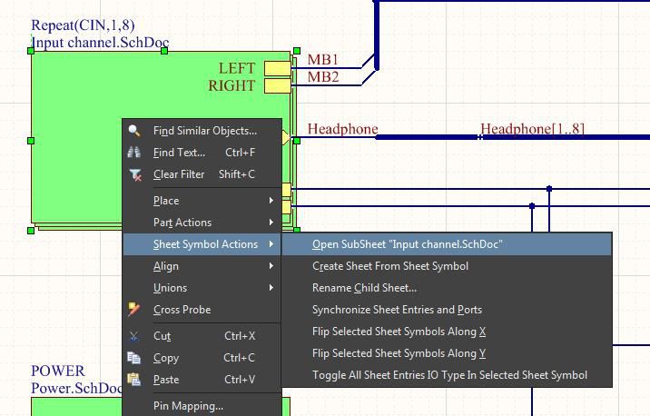
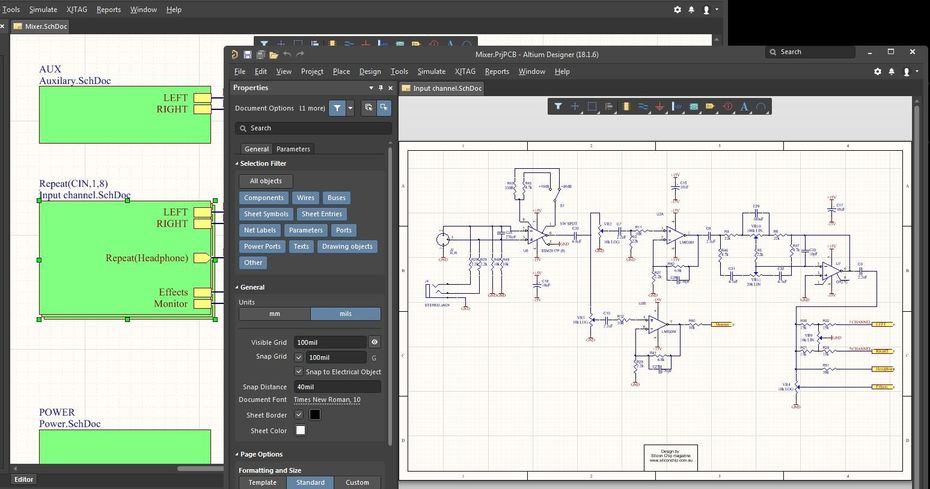
There is a lot of joy in creating a schematic. Placing and connecting the netlist together so that their logic flows naturally can give you a feeling of great accomplishment. Using a hierarchical schematic design flow to organize a larger schematic makes it even better. By including a top hierarchical sheet in your schematic, you can represent the circuit design with a logical hierarchical block that represent the actual lower sheets of circuitry in the schematic.
The problem is that a lot of designers will avoid using hierarchy at any cost because it can be difficult to work with. I know this because I used to be one of those design engineers.
Depending on the PCB CAD system that you are using, there may be a lot of work ahead of you to create a hierarchical design. Even though it can be painful to spread a large design file through a lot of sheets in a flat schematic, many users will view this as the lesser of two evils in order to avoid working with hierarchy.
It’s a shame too because the circuitry flow can often be better represented in a hierarchical design, and a design with repeated circuitry can really benefit from using a multi-channel hierarchical approach. Multi-channel hierarchical designs can add an even higher level of complication to the schematic creation process.
Some PCB layout systems today though that make the job of schematic design with hierarchy a whole lot easier than it used to be. These systems can go a long ways towards easing the traditional pain of working with schematic hierarchy and make it so that you will look forward to working with it.
The Pain of File Management in Hierarchical Schematic Design Systems
One of the biggest problems that I have had working with a hierarchy in the past was with working with CAD systems that required a lot of file manipulation. This has often meant keeping track of the files created for sub-sheets in a hierarchy and then making sure to connect to the right sheet and that it was in the expected file folder location. I’m sure that I haven’t been the only designer to blow up my schematic after mismanaging files and moving something I shouldn’t have.
Another issue is in having to configure all of these files to work together. This usually means keeping careful track of net names and sheet information. It also means that somewhere along the line there will be configuration files that have to be constantly edited in order to hold everything together. What I always longed for was a system that wasn’t so bulky and cumbersome to work with.

Multi-Channel Schematic Designs Only Increases the Pain
Using these systems was difficult enough working with a regular hierarchical design, but when it came to repeating blocks of circuitry in a multi-channel design it became a nightmare. A multi-channel design can be very difficult and complex and you need to be careful about the following:
Even more care must be taken to correctly manage the files and configurations of the sub-sheets then in a regular hierarchical design.
Passing properties correctly through multi-channels can be difficult.
It often takes multiple passes through the synchronization process in order to completely pair the schematic up with the PCB.
You must be very careful with net names so that they don’t get confused in the hierarchy of the multi-channels.
The problem boils down to this: if a new task becomes too daunting then the users will go back to the old way of doing things. In the case of schematic design, this means that you will see more flat schematics instead of hierarchical designs. Designers know that flat schematics are more bulky, less intuitive, and take more time to create and work with. They will default to creating a flat schematic because there is less chance of them making a mistake.
What we need is a schematic capture tool that eases the pain of creating a hierarchical schematic.

The Way a Hierarchical Schematic Design System Should Work
The answer to our pain is in a schematic capture system that has its basis in a PCB CAD design platform that is based on a unified data model. With the data already prepared to work together throughout the design, it is much easier for the connectivity to work in a hierarchical design.
This reduces the workload on the designer in managing files and configuration settings and makes the process of creating a hierarchical schematic more intuitive. With designers routinely working in hierarchical schematics, it will promote more logical looking schematics, encourage team design, and reduce the workload with design reuse.
We have found that Altium Designer® gives us the schematic capture system that works the best for hierarchical designs. You can easily create a child design from a new block symbol, or pull in an existing design into your current session and associate it with block symbol. Altium Designer also lends itself well to multi-channel hierarchical design and design reuse. If you haven’t tried it yet you should take a look at it. With Altium Designer as your PCB design software, you will be able to see the ways that hierarchical design will save you time and effort.
Would you like to find out more about how Altium Designer can help you to open up a whole new world of hierarchical schematic design? Talk to our expert.
