Every PCB design project starts with a stackup that has clearly defined signal and plane layers. Make sure you choose the right stackup for your design and make sure you design your stackup to comply with your fabricator’s requirements. A 4-layer PCB stackup may seem simple, but it needs to be designed with the right layer arrangement to ensure correct fabrication and impedance. Utilize the right PCB design software that helps you build the best 4-layer stackup.
A PCB design software package with stackup design features for professional PCB layout engineers.
Whenever you start a PCB design project, it’s likely that your last instinct is to contact your fabricator about their stackup requirements. However, you would be surprised at the number of PCB stackups that need to be modified before beginning full-scale production. Every PCB stackup needs to be built to consider fabrication capabilities, available materials, and target impedance, and it’s your fabricator’s job to provide the PCB stackup specification for your layer count.
A 4-layer PCB stackup is the most common multilayer PCB stackup used in modern electronics. This stackup is rather simple and can be reliably fabricated as long as the basic layer thickness and layer arrangement requirements are met. Instead of guessing at the right layer count, dielectric constant, and loss tangent to define in your PCB, use the best PCB design tools in Altium Designer to implement your fabricator requirements. Altium Designer provides the essential tools needed to create a PCB 4-layer stackup in standard rigid boards, rigid-flex boards, and multilayer board assemblies.
Defining a 4-layer Stackup for Your Printed Circuit Board
Because 4-layer PCBs are so common in many products, designers should have an idea of how to use and design a 4-layer stackup. With the right design tools and guidance from your PCB fabricator, it’s easy to design a 4-layer PCB stackup.
The image below shows a standard 4-layer stackup used by most fabricators. This stackup uses a thick core layer in the center of the board covered with two thinner prepreg layers. The two inner layers are often used for power and ground nets, while the surface layers are used primarily for signals and for mounting components. In addition, the outer layers will be covered in solder mask with exposed pads to provide a spot to mount SMD and through-hole components. Finally, through-hole vias are normally used to provide connections between layers.
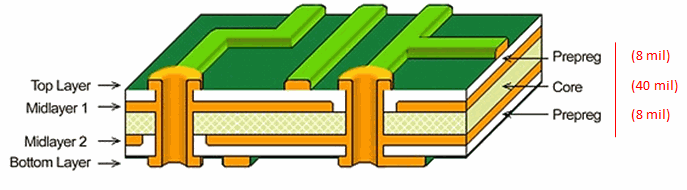
Alternative 4-layer PCB stackups will use a prepreg sheet on the central layer and two core laminates on the outer layers, sometimes all with the same thickness. The above arrangement may have slightly different thicknesses, but this is only critical when working with impedance-controlled traces and routing. Otherwise, the above stackup is very versatile, and it is used in everything from simple digital boards to computer motherboards and fast DDR memory sticks.
Easily Define the Form Factor with Circuit Board Shape
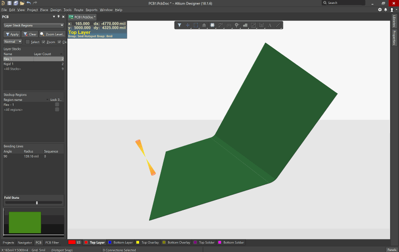
After designing the stackup for your 4-layer board, it’s time to define the board shape before component placement. When working in Altium Designer’s PCB Editor, you can define the board shape area available for components and routing. One option is to import a DXF file into a mechanical layer and use this to define the board shape. Alternatively, you can use the board shape editor to customize the dimensions and shape of your PCB.
The Board Shape tool also allows you to split the printed circuit boards into multiple board regions and place bending lines on a flex board region. You can also use Board Shape to split power planes and define the boundaries of the power planes. As you work with rigid-flex designs, you can balance the mechanical and electronic design areas by using the surface of an imported 3D STEP model to redefine the board shape.
Make sure to select the right dielectric materials for your PCB and set the thickness needed to ensure you comply with your fabricator’s design requirements.
One important point to understand is the difference between core and prepreg materials in any PCB stackup.
If you need more advanced capabilities than what you’ll find in FR4 laminates, there are many alternative PCB materials you can use in your design.
Support for Rigid-flex PCB Designs
The IPC-6013 standard defines four types of stackups for flex and rigid-flex boards:
Type 1 – Single-layer Flex: Uses one conductive layer uncovered on one side or laminated between insulating layers.
Type 2 – Double-layer Flex: Uses two conductive layers with plated through holes.
Type 3 – Multilayer Flex: Also uses plated through-holes between layers with conductor allowed on all layers.
Type 4 – Multilayer Rigid-flex: Combines rigid and flexible layers in the rigid section with an exposed flexible section and conductors on the rigid layers.
Because rigid-flex multilayer boards have different 4-layer PCB stackup requirements, design teams must define multiple layer stacks along with the rigid and flexible zones of the printed circuit board. Each zone or board region associates with a specific layer stack.
Altium Designer Offers Advanced PCB Layer Stack Management
Altium Designer allows the definition of multiple stacks for rigid-flex designs. An overall master layer stack defines the total set of available layers for the design. You can define any number of sub-stacks from the available master stack layers. Layer Stack Manager allows design teams to carefully define bending regions when establishing the overall shape of the rigid-flex board.
Altium’s Layer Stack Manager allows designers to configure the layers of a printed circuit board. While using the Layer Stack Manager, you to add, merge, remove, and configure the layer stacks. After the Layer Stack Manager defines the material and mechanical requirements of the layers, materials, thicknesses, and dielectric constants, Altium Designer uses the Layer Stack Table to graphically document the layer configurations.
You can define the layer properties while consulting with your fabricator. Layer properties extend across the entire layer and across all associated stacks. All mechanical layers appear after the physical layers. You can use the Layer Stack Table documentation to lessen the complexity of rigid-flex layer stack structures.
Rigid-flex PCBs provide many advantages, but they aren’t always needed and they require advanced design circuit board software like Altium Designer.
Some materials are compatible with each other as defined in IPC slash sheets, including rigid-flex and flex materials.
Some flex and rigid-flex PCBs are designed for either static or dynamic bending, and the need for repeated bending should be included in the flex stackup design.
Calculate the Correct Routing Impedance for a PCB Layout
After building the PCB layer stack for your 4-layer stackup or more advanced board, you may need to set a target impedance for specific traces. With the complete set of PCB design rules in Altium Designer, users can take control of all aspects of their layout and routing. This includes clearances between important features like vias, pads, and polygons, as well as defining feature sizes to ensure signal integrity and manufacturability.
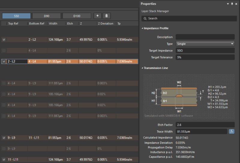
The PCB stackup will determine the impedance of conductors routed on the surface layer. The integrated field solver from Simberian in Altium Designer provides accurate impedance calculations without using an external application. The calculated width and clearances determined in the layer stack design editor can then be set as an electrical design rule for layout and routing. The target impedance required in the board will be enforced throughout routing to ensure accurate layout, including when routing through vias and applying teardrops to connect to large pads.
When you route the Circuit Board and change the number of layers, Altium Designer automatically adjusts the track width to the size that matches the impedance. The Signal Integrity command found within the Altium Designer PCB Editor Tools menu allows you to use the material properties established through the Layer Stack Manager and the actual widths of the routes to check for impedance mismatches and reflection issues.
Real-time BOM Management Assists with PCB Manufacturing
Altium Designer’s advanced design toolset is available alongside a complete set of manufacturing and documentation features. ECAD toolsets are accessible alongside your bill of materials (BOM) that shows all the components used in the PCBA. Information in the BOM feeds into the CAD system and becomes part of the PCB layout and schematics, and manufacturing preparation features will pull this data to help create fabrication and assembly files.
The unified environment offered within Altium Designer combines access to those tools with the capability to seamlessly communicate with layout, simulation, and rules checking features. By placing all these features in a single application, designers can manufacturer their 4-layer PCBs with confidence.
Use the best design features that help guide you throughout the PCB design process and help you build advanced electronics in a single program.
The powerful mechanical design tools in Altium Designer are built to help you create rigid-flex PCBs and flexible PCBs for advanced applications.
Every Altium Designer user has access to the Altium 365 platform, the only managed cloud platform for sharing and collaboration on complex design projects.
Only Altium Designer gives its users a complete set of layer stack design features to build a 4-layer stackup or more advanced circuit boards. All Altium Designer users can easily prepare documentation for their circuit boards and send their design data in for manufacturing with a single application. No other PCB design software company gives its users this many features for successful circuit board design.
Altium Designer on Altium 365 delivers an unprecedented amount of integration to the electronics industry until now relegated to the world of software development, allowing designers to work from home and reach unprecedented levels of efficiency.