Every PCB will need some holes, vias, slots, and other features that are defined in a PCB layout. These features need to be reflected in fabrication documents, and designers need tools to help them automate this process of creating documentation directly from their designs. It’s easy to keep track of your holes, vias, electrical behavior, and much more in Altium Designer, the industry’s top PCB design application for professional design engineers. With Altium Designer, you can do all of this and more, and all within a single software platform.
A PCB design software package that generates manufacturing and assembly instructions in industry-standard file formats.
With the number of PCB design software programs and utilities out there, it can be difficult to choose the program that will work best for you. Your CAD software should help you stay productive in all of your design projects, and it should help you get your designs into manufacturing. Part of ensuring successful manufacturing involves placing the correct fabrication notes into your documentation, which should be pulled directly from your design data.
An important part of PCB fabrication is placing drill holes with standard drill bit sizes in the board to provide through-hole component solder points, mounting holes, and via holes in your circuit board. Knowing something about the standard PCB drill sizes and how a drill hole is defined in your PCB design software will help ensure your fabrication run is successful and has high yield. The right PCB design software can help ensure your next design is manufactured correctly with the right PCB drill sizes.
PCB Drill Sizes and How They Are Fabricated
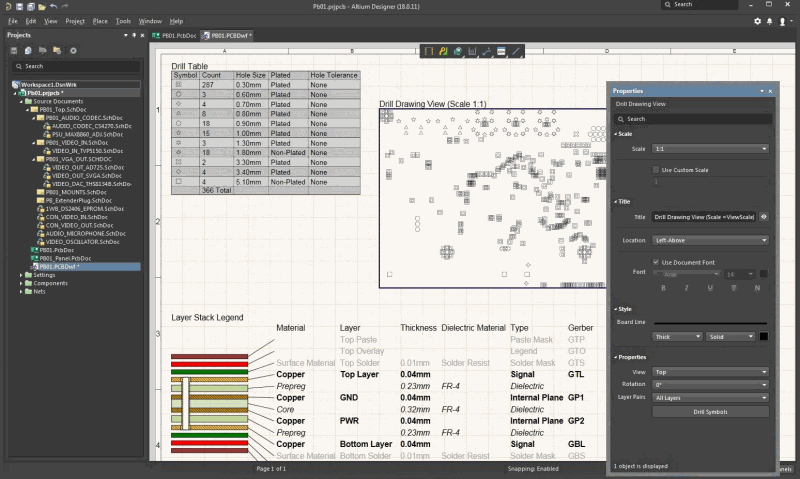
The drill holes in a PCB are placed with standard drill bit sizes after a board stackup is fabricated but before the board is plated. The drill locations and drill bit sizes are indicated in a drill table in the PCB fabrication documents. The drill locations are also defined in the Gerber files and an NC drill file, which are then used with a NC drill machine to place holes.
The standard drill bit sizes are in metric and Imperial gradations. Drill sizes in Imperial units reach down to fractions of an inch, often being measured in mils for mechanical drilling. Metric drill sizes are also very small and come in standard sets. No matter how small a drill hole needs to be, the drill hole and pad need to be designed together to ensure high yield, reliability, and assembly.
Pad Diameter Needed for Your PCB Drill Bits
According to the IPC-2221A Standard Specification, your drill bit size depends on the pad size, and vice versa, in order to ensure reliability and yield. The pad size needed to support a drill bit depends on the size of the annular ring placed around a hole, the hole size, and the tolerance:
Minimum Annular Ring = (Min. Ring Border) * 2 + (Tolerance Allowance) + (Hole Size)
Minimum Annular Ring on the Inner Layer: 0.1 mm
Minimum Annular Ring on the Outer Layer: 0.05 mm
The tolerance value will depend on the IPC Producibility Levels. Your tolerance allowance should never be smaller than 0.6mm for Level A, 0.5 mm for Level B, and 0.4 mm for Level C.
These drill specifications are extremely important when you move to manufacturing your printed circuit board. When you work with the best design software, it’s easy to define customized vias, tooling hole features, and drilling specifications that translate directly into your manufacturing outputs.
The top-notch CAD tools in Altium designer let you build the best quality layouts with customized pad/via templates that are easily placed in your PCB layout.
Once you set your via size, Altium Designer gives you features to optimize your nets, verify trace clearance, and route between layers.
Generating your manufacturing outputs is easy in Altium Designer. Your layout and fabrication specifications sync directly to your manufacturing outputs and are exported in standard file formats, including drill tables in your NC drill files and Gerbers.
 Define and align your mounting holes and vias in Altium Designer
Take Control of Your Via and PCB Drill Size Specifications
Once you’ve placed your pads and vias, and you’ve defined your hole sizes, there is still more work to do. You’ll need to define drilling steps for your vias, conductive and non-conductive fill options, any via tenting, and connections to other layers in the PCB stackup. Altium Designer has all the tools you need to define your via structures and includes the fabrication and drill holes in your manufacturing outputs. Keeping your information clear, precise, and documented will keep your production process running forward.
With all the design and routing features required to make your PCB work properly, it is understandable that folks tend to overlook fabrication and PCB manufacturing. An integrated design package gives you the power to design top-quality printed circuit boards and define your manufacturing specifications within a unified environment. Aspect ratios, board thickness, annular rings, and soldering can all be arranged beforehand in strong PCB design software.
Customizing Drill Steps for Your Vias Is Easy With Altium Designer
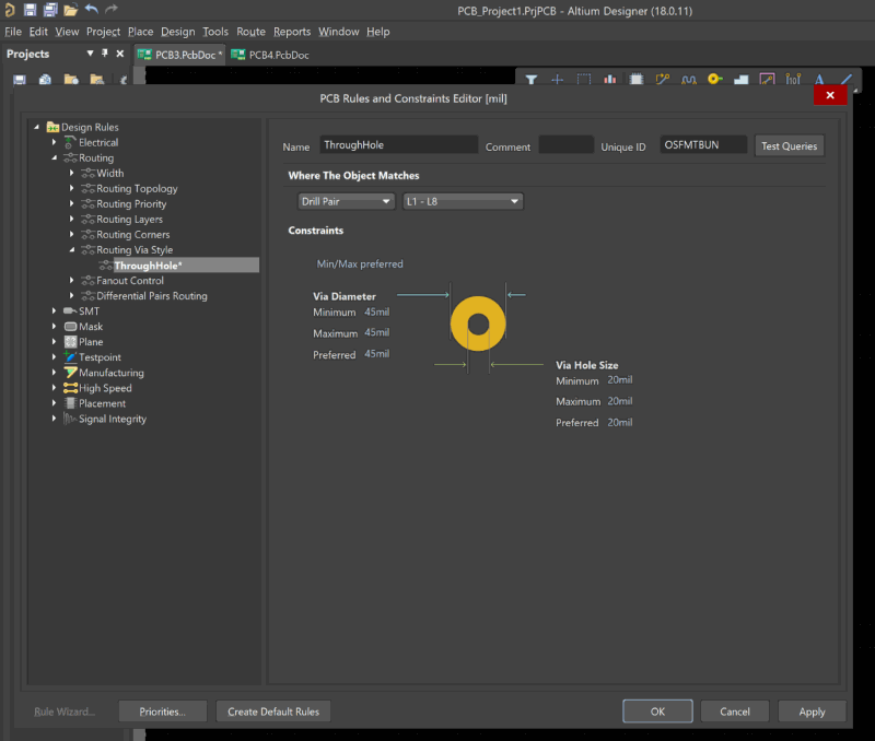
Perhaps the most important routing features in a multilayer PCB are vias. Your vias are what let you route between each layer in your board. Whether you’re placing via-in-pad, through-hole vias, blind vias, or buried vias, you will need to define drill diameter and depth in each layer. Altium Designer gives you all the tools you need to customize your via sizes and specify how you want them placed in your board.
Altium Designer gives you the ability to define your drill pairs while configuring your layer stackup, and your vias will automatically match specific drill pairs in your PCB stackup.
Altium Designer lets you export your drilling instructions in the popular Gerber and Excellon 2 file formats. The CAM Editor in Altium Designer also supports traditional file formats (e.g. Gerber, ODB++, Aperture List Files (*.lst), and NC Drill/Excellon 2) that are used to build CAM documents.
Altium Designer makes it easy to define depth drilling and backdrill vias for high-speed PCB interconnects.
Defining Drill Hole Sizes in Your Manufacturing Outputs
Your drill specifications in your PCB layout data need to be reflected in your PCB fabrication instructions in standard file formats. Preparing a design for circuit board manufacturing shouldn’t require manually placing the machining steps in your design documentation. Instead, Altium Designer can help you create your CAD/CAM drawings, Gerber files, and Excellon drill files. Other software companies will try to sell you separate software programs for your printed circuit board’s separate needs, but Altium Designer gives you all of these capabilities within a single software package.
Altium Designer gives you the capability to define your mounting hole and backdrill hole diameters within a convenient interface. Drill bit diameters are easily specified in a drill table in a mechanical layer in your PCB layout, and this can be instantly transferred to your PCB fabrication documents. Altium Designer also supports standard imperial and metric drill bit sizes, or you can enter custom PCB drill sizes. Altium Designer also lets you define routed or milled holes in your board, giving you serious flexibility and customization power.
Altium Designer Supports Industry Standard File Formats
When you prepare your fabrication files for release to your manufacturer, Altium Designer will show your drill table with all hole sizes in your Gerber files and other fabrication documents. It’s easy to define the drill table in a layer in your CAD data, generate drawings with your PCB drill sizes data, and export Gerber files in RS-274-X and X2 formats. Altium Designer takes the headache out of planning for manufacturing and helps ensure your fabrication files are correct.
When you need to specify all the copper features and drill sizes in your PCB stackup and layout, use the comprehensive set of design tools in Altium Designer.
Manufacturing and multiboard assembly are easy with Altium Designer’s integrated fabrication and assembly utilities.
Every Altium Designer user has access to the Altium 365 platform, the only cloud platform that lets you instantly release your design and production data through Altium Designer or on the web.
With the best PCB design software, it’s easy to define PCB drill sizes for holes and vias in your PCB layout. Once you’re ready to start PCB fabrication, you can prepare your design for production with a complete set of documentation tools. Only Altium helps you stay at the cutting-edge of technology while guiding you through the manufacturing process in a single application.
Altium Designer on Altium 365 delivers an unprecedented amount of integration to the electronics industry until now relegated to the world of software development, allowing designers to work from home and reach unprecedented levels of efficiency.
We have only scratched the surface of what is possible to do with Altium Designer on Altium 365. You can check the product page for a more in-depth feature description or one of the On-Demand Webinar.